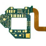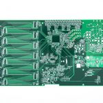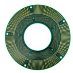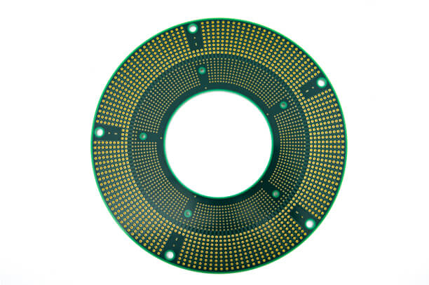
Multilayer PCB
Manufacturing multilayer PCB up to 64 layers, IPC III Standard, Multilayer Rigid PCB, Multilayer Flex PCB, Rigid-flex Board, hybrid PCB.
Over the past decade, the production of complex multi-layer PCB has been the cornerstone of The competitive advantage of FastLink electronics. We continue to invest in RESEARCH and development, equipment and engineering expertise to improve our technology and capabilities. Fastlink Electronics provides NPI with early prototypes of new products to help achieve high volume production. We do all the necessary operations in a production deployment environment to ensure you produce the quantity you need in the shortest possible time.
What Are The Applications Of Multilayer PCBs?
Multilayer printed circuit boards (PCBs) bring you greater flexibility, allow for greater circuit density, and reduce board size. They are widely used in various fields:
Computers and Laptops
Telecommunications Equipment – Mobile Phone, Tablets, and other Hand Help Devices
File server and Data storage
Signal transmission, mobile phone repeaters, GPS
Satellite
Medical Equipment: Testing, X-Ray, Heart Monitor, CAT Scan
Industrial Equipment
Atomic and Nuclear Systems
Military and Defense Equipment
Automotive
Aerospace
Anywhere, where complex Circuitry is needed.
Benefits of Multilayer PCB
01.
Increased Functionality And Capabilities
By compounding multilayer boards, you can effectively increase the functionality and capabilities of printed circuit boards. With more layers, you can fit more circuits and lines onto the board.
02.
More Flexible
Can be made rigid or flexible – These multi-layer PCB can be made rigid or flexible configurations, depending on your requirements. However, the more layers you add to the board, the less flexible it becomes.
03.
Smaller Sizes
This saves space when you stack layers on top of each other. Multiple layers allow you to have a higher capacity with a smaller footprint, which may benefit smaller devices.
04.
Lighter Weight
Due to the layered configuration of these PCB boards, it does not require a separate PCB connector. This simplifies the manufacturing process, which not only saves space, but also reduces the overall weight of the board.